M9OMS VLDO V2.1 — Optional Modification
An optional modification to the V2.1 board, for builders who wish to implement it. A 1 µF capacitor is added between pin 5 of the voltage reference and ground, which eliminates a slight rise above target observed at the 9 V setting (see the previous page). This increases startup time, with no adverse effect on safety or operation. This page records the captures, verifying the addition of this capacitor. A 100 nF capacitor can be tried - though this value has not been tested.
Measurements by CR7BTQ (September 2026), on a single V2.1 board.
Product page: M9OMS VLDO V2 — RF-quiet power supply for QRP Labs QMX
Test setup and conditions
The setup is identical to that used for the main oscilloscope measurements. The only variable is the addition of the 1 µF capacitor between pin 5 of the voltage reference and ground. The captures in sections 1 and 2 were taken at the 9 V jumper setting.
1. Startup timing
TEK00053 — Output rise to settled value
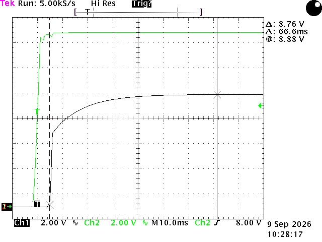
Measured from the first increase in output until settling at its final value, the cursor interval is 66.6 ms, with the settled output read at 8.88 V.
TEK00054 — Input applied to settled output
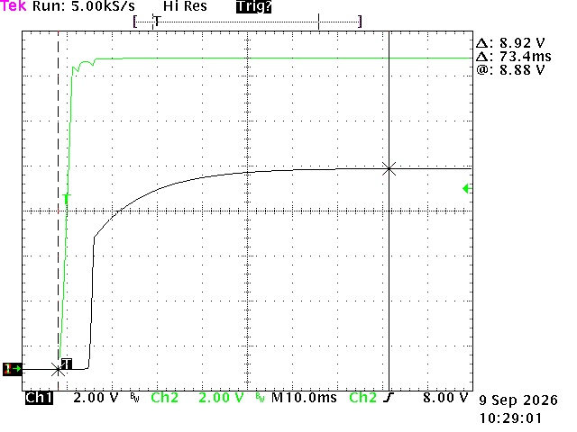
Measured from the point at which the input is applied, the interval is 73.4 ms. This figure includes the input transition and will therefore vary with the rate of rise on the input.
2. The output rise
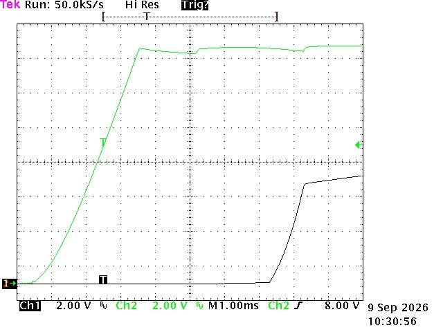
TEK00055 — Output rise, 1.00 ms/div
TEK00056 — Output rise, 200 µs/div
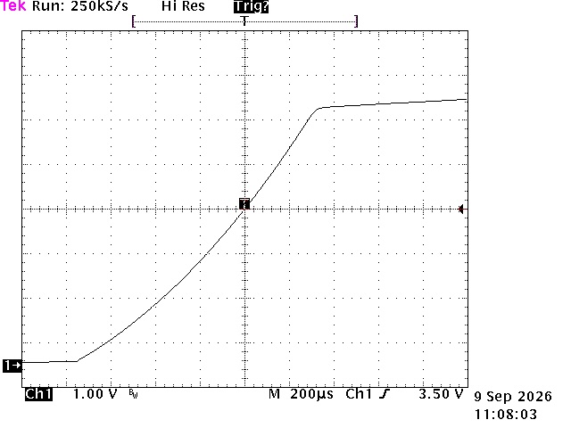
At these timebases the rise is smooth and controlled throughout. The output reaches approximately 6 V in roughly 1 ms - which is considered to be a fast startup time. A QMX and QMX+ CPU would have powered up in this timeframe, and the final settled voltage is reached shortly after that. This is unlikely to affect the PA during normal operation - the PA isn’t active when powering up.
3. 12 V setting
The 12 V setting was observed on the oscilloscope but not captured. It follows the 9 V setting, the shape of the ramp being consistent across output voltages. The output rises quickly to around two-thirds of the final output voltage, then more slowly until it reaches the final value, in a way that resembles a logarithmic curve.
4. How to implement this
Either method is acceptable; choose whichever suits your ability.
Option 1 — SMD capacitor to pin 5 and board ground
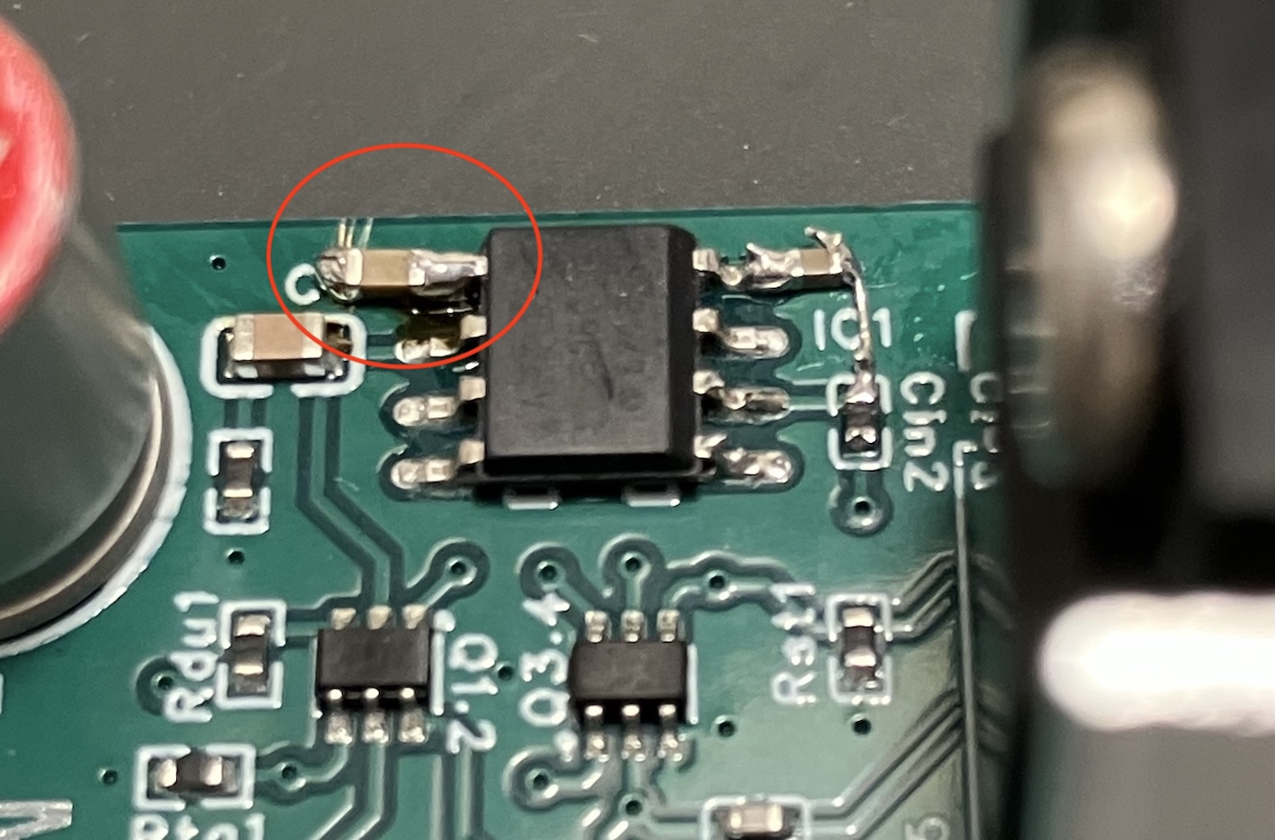
Remove a small area of solder mask to expose board ground, then place and solder the 1 µF capacitor between pin 5 of the voltage reference and that point. The photograph above was taken on a prototype board.
Option 2 — THT capacitor between pin 5 and the reference ground pin
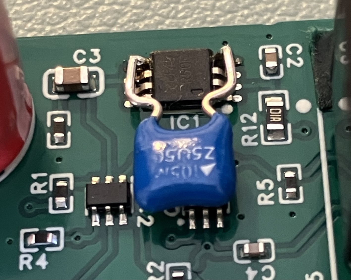
Solder a through-hole capacitor directly between pin 5 of the voltage reference and its ground pin. The photograph above was taken on a final production board.
Take care not to bridge any pins on IC1 - they have a fine pitch.
Oscilloscope measurements: CR7BTQ, September 2026. See the project README for design rationale and the full specification table.