VLDO V1
Further development has moved to VLDO V2. Independent measurements and characterisation make V2 the recommended choice for new builds and applications. The BOM and Gerber files for this earlier design are provided here as an open hardware reference.
SEE NOTES BELOW.
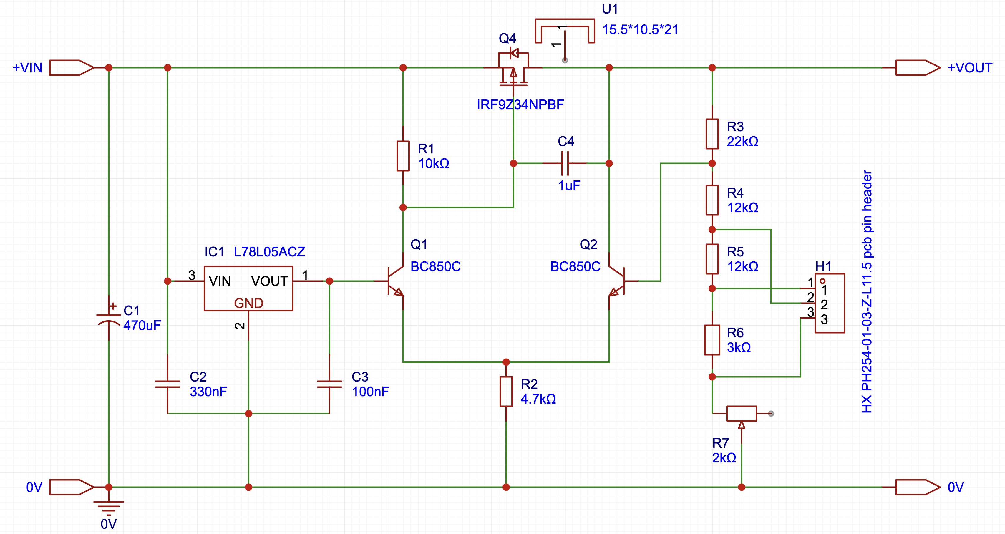
Notes
Based on G4COL’s schematic, with the following changes (final, V1.2 revision): 1- Additional input bypass capacitor. 2- Voltage selection ladder & trim potentiometer. 3- SMD components.
PCB dimensions: 65mm x 20.5mm x 25mm. 3D printed housing: https://www.thingiverse.com/thing:7246700
BOM, Gerber and CPL are shared on a CC BY-NC-ND basis. Verify schematic before committing to fabrication.
Download V1 BOM & Gerber here:
Additional materials required:
- 1x 2.54mm shunt.
- 1x TO-220 isolation kit (including M3 machine screw).
Why CC BY-NC-ND?
The BOM, Gerber and CPL files correspond to a validated design configuration. Maintaining the original component selection helps preserve the measured performance of this implementation under the tested conditions.
Component changes may affect stability. In particular, changes affecting pass-device capacitance, amplifier drive capability, feedback network impedance, and reference-node behaviour should be treated carefully.
Although the BOM reflects the validated component set for this implementation, stability should still be verified. Component tolerances, substitutions, layout differences, and other factors may affect performance.
Parameters
- Input voltage: 9–18 V DC
- Output voltage options: approximately 9.0 V / 12.0 V / 13.6 V
- Voltage drop: typically 0.04–0.4 V at 1 A (depending on input voltage)
- Maximum continuous output current: 2 A
- Output trim via R7
- PCB dimensions: 65 × 20.5 mm (25 mm height including heatsink)
Thermal considerations:
The onboard heatsink supports approximately 1.5 W of continuous power dissipation. Higher dissipation requires additional cooling, such as mounting the TO-220 pass device to a larger heatsink or suitable metal enclosure. Electrical isolation must be maintained, as the device tab is connected to the output rail.