M9OMS VLDO V2 — Bench Measurements (Dropout, Line/Load Regulation & Thermal Data)
Measured DC and thermal performance of the M9OMS VLDO V2 regulator. This page records hardware results that supplement — and progressively replace — the simulation figures in the main specification table.
Measurements by Stan Dye, KC7XE (June 2026), on a single production-representative V2 board supplied by M9OMS. Method follows Stan’s characterisation of the first M9OMS V1 prototype, shared on the QRP Labs group. Spot-checks at a few operating points by CR7BTQ and M9OMS, on separate same-batch boards in different locations, returned figures consistent with this dataset — indicating the results are representative of the batch rather than a single-unit or single-lab artifact.
Full evaluation by KC7XE downloadable here.
Product page: M9OMS VLDO V2 — RF-quiet power supply for QRP Labs QMX
Test method and conditions
- All voltages measured at the VLDO board terminals. The supply was raised as load increased to hold Vin at the stated value, removing lead-resistance drop from the results. Repeating these sweeps without compensating for supply-lead drop will give lower apparent Vout at high current.
- Single-sample dataset. The full tabulated sweeps are from one board. Spot-checks on two further same-batch boards (CR7BTQ, M9OMS, different locations) agree with these figures; the board has not been temperature-cycled, so treat the results as representative rather than guaranteed limits.
- Load range. Sweeps cover 0–4 A. The 2 A column is the rated continuous maximum; the 4 A column is included for reference only (beyond rating).
- Application focus. Emphasis is on QMX / QMX+ use — roughly 100 mA receive and ~1 A transmit — so thermal testing concentrates on that range.
- Thermal setup. 20 °C ambient, still air, supplied heatsink only, board open on the bench (no enclosure). Thermocouple fixed between the heatsink fins.
Output-voltage setup
The jumper selects one of three nominal outputs, fine-trimmed with R7. The trimmer was
set once for 9.00 V at 100 mA; the other two settings were then left untouched, which
landed them close enough that no per-setting re-trim was needed:
| Jumper setting | Output at 100 mA |
|---|---|
| 9 V | 9.00 V (trimmed reference) |
| 12 V | 12.04 V |
| 13.8 V | 13.79 V |
DC performance at a glance
| Parameter | Measured | Condition | Simulated spec |
|---|---|---|---|
| Dropout | <100 mV | 1 A, at board terminals | < 100 mV @ 1 A |
| Dropout | <200 mV | 2 A | ~200 mV @ 2 A (est.) |
| Load regulation | ~20 mV / ~40 mV | 0.1→1 A / 0.1→2 A, in regulation | ~20 mV / ~40 mV |
| Line regulation | ≤ ~8 mV/V | 100 mA and 1.0 A, regulation onset → max Vin, worst case (12 V setting) | < 5 mV |
| Minimum input | usable to 7 V | rises with load below ~7 V (see note) | 8 V (continuous) |
| No-load float | +30 mV ±10 mV | output open vs. lightly loaded | - |
Measured dropout sits comfortably inside the simulated < 100 mV figure, and line and load
regulation track the simulation closely. Because everything is referenced to the board
terminals, these numbers reflect the regulator itself rather than wiring resistance.
Line and load regulation
Each setting is shown twice: a full sweep across the input range, then a zoomed view of the regulation knee where the millivolt-scale detail lives. The dashed grey line marks Vout = Vin (the ideal “no headroom” boundary); below the knee the output tracks the input less the dropout, and above it the output holds flat.
9 V output
| Vin | 0 mA | 100 mA | 500 mA | 1000 mA | 1500 mA | 2000 mA | 4000 mA |
|---|---|---|---|---|---|---|---|
| 6.50 | 6.50 | 6.49 | 6.44 | 2.50 | 0.00 | 0.00 | — |
| 7.00 | 7.00 | 7.00 | 6.98 | 6.96 | 6.95 | 6.94 | 6.86 |
| 7.50 | 7.50 | 7.50 | 7.49 | 7.48 | 7.46 | 7.44 | 7.38 |
| 8.00 | 8.00 | 8.00 | 7.99 | 7.98 | 7.96 | 7.95 | 7.92 |
| 8.90 | 8.90 | 8.90 | 8.89 | 8.88 | 8.86 | 8.84 | 8.78 |
| 9.00 | 9.00 | 9.00 | 8.99 | 8.98 | 8.97 | 8.95 | 8.88 |
| 9.10 | 9.03 | 9.00 | 8.99 | 8.98 | 8.97 | 8.97 | 8.93 |
| 9.50 | 9.03 | 9.00 | 8.99 | 8.98 | 8.98 | 8.98 | 8.95 |
| 10.00 | 9.04 | 9.00 | 8.99 | 8.99 | 8.98 | 8.98 | 8.96 |
| 11.00 | 9.04 | 9.01 | 9.00 | 9.00 | 8.99 | 8.99 | 8.97 |
| 12.00 | 9.05 | 9.01 | 9.00 | 9.00 | 9.00 | 9.00 | 8.98 |
| 13.00 | 9.06 | 9.02 | 9.01 | 9.00 | 9.00 | 9.00 | 8.98 |
| 14.00 | 9.04 | 9.00 | 9.00 | 9.00 | 9.00 | 9.00 | — |
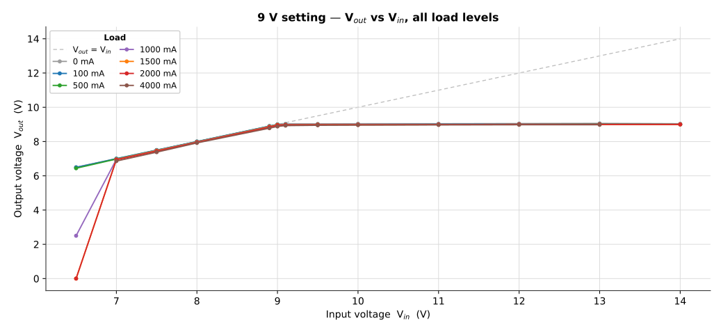
9 V setting — full input sweep, all load levels.
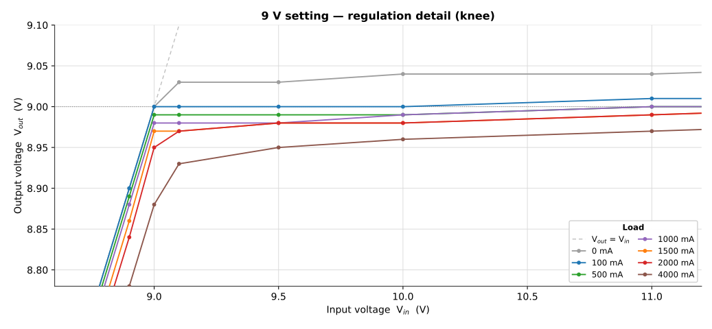
9 V setting — regulation knee in detail.
12 V output
Measured at the 12 V jumper position, trimmed baseline 12.04 V at 100 mA.
| Vin | 0 mA | 100 mA | 500 mA | 1000 mA | 1500 mA | 2000 mA | 4000 mA |
|---|---|---|---|---|---|---|---|
| 6.50 | 6.50 | 6.49 | 6.44 | 2.50 | 0.00 | 0.00 | — |
| 7.00 | 7.00 | 7.00 | 6.98 | 6.96 | 6.95 | 6.94 | 6.86 |
| 7.50 | 7.50 | 7.50 | 7.49 | 7.48 | 7.46 | 7.44 | 7.38 |
| 8.00 | 8.00 | 8.00 | 7.99 | 7.98 | 7.96 | 7.95 | 7.92 |
| 9.00 | 9.00 | 9.00 | 8.99 | 8.98 | 8.97 | 8.95 | 8.88 |
| 10.00 | 10.00 | 10.00 | 9.99 | 9.98 | 9.97 | 9.96 | 9.85 |
| 11.00 | 11.00 | 11.00 | 10.99 | 10.98 | 10.97 | 10.96 | 10.88 |
| 11.90 | 11.90 | 11.89 | 11.88 | 11.87 | 11.86 | 11.85 | 11.74 |
| 12.00 | 12.00 | 11.99 | 11.98 | 11.97 | 11.96 | 11.95 | 11.84 |
| 12.10 | 12.05 | 12.02 | 12.01 | 12.00 | 11.99 | 11.98 | 11.91 |
| 12.20 | 12.07 | 12.02 | 12.01 | 12.00 | 12.00 | 11.99 | 11.93 |
| 12.50 | 12.07 | 12.03 | 12.02 | 12.01 | 12.00 | 12.00 | 11.96 |
| 13.00 | 12.08 | 12.04 | 12.03 | 12.02 | 12.01 | 12.01 | 11.96 |
| 14.00 | 12.07 | 12.03 | 12.02 | 12.01 | 12.01 | 12.01 | 11.96 |
| 15.00 | 12.08 | 12.04 | 12.02 | 12.02 | 12.02 | 12.02 | 11.97 |
| 16.00 | 12.09 | 12.05 | 12.03 | 12.03 | 12.03 | 12.03 | 11.97 |
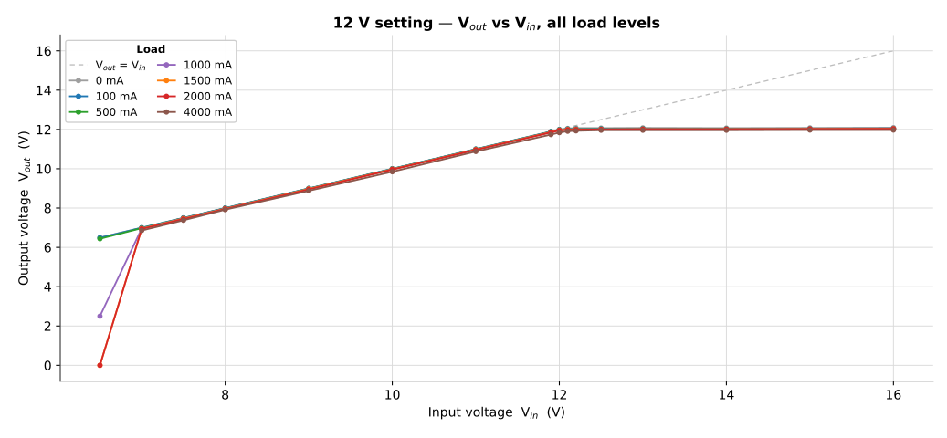
12 V setting — full input sweep, all load levels.
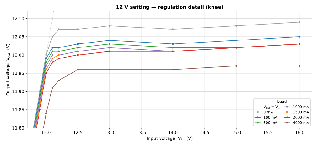
12 V setting — regulation knee in detail.
13.8 V output
Measured at the 13.8 V jumper position, trimmed baseline 13.79 V at 100 mA.
| Vin | 0 mA | 100 mA | 500 mA | 1000 mA | 1500 mA | 2000 mA | 4000 mA |
|---|---|---|---|---|---|---|---|
| 6.50 | 6.50 | 6.49 | 6.34 | 1.90 | 0.00 | 0.00 | — |
| 7.00 | 7.00 | 7.00 | 6.98 | 6.96 | 6.95 | 6.94 | 6.82 |
| 8.00 | 8.00 | 8.00 | 7.99 | 7.97 | 7.97 | 7.96 | 7.87 |
| 9.00 | 9.00 | 9.00 | 8.99 | 8.97 | 8.97 | 8.96 | 8.88 |
| 10.00 | 10.00 | 10.00 | 9.99 | 9.97 | 9.97 | 9.95 | 9.86 |
| 11.00 | 11.00 | 11.00 | 10.99 | 10.97 | 10.97 | 10.95 | 10.89 |
| 12.00 | 12.00 | 12.00 | 11.99 | 11.97 | 11.97 | 11.96 | 11.91 |
| 13.00 | 13.00 | 13.00 | 12.99 | 12.97 | 12.97 | 12.95 | 12.91 |
| 13.60 | 13.60 | 13.60 | 13.59 | 13.58 | 13.57 | 13.56 | 13.48 |
| 13.80 | 13.80 | 13.77 | 13.76 | 13.75 | 13.73 | 13.72 | 13.68 |
| 14.00 | 13.82 | 13.79 | 13.77 | 13.76 | 13.76 | 13.75 | 13.71 |
| 15.00 | 13.82 | 13.79 | 13.77 | 13.76 | 13.76 | 13.76 | 13.73 |
| 16.00 | 13.82 | 13.79 | 13.77 | 13.77 | 13.77 | 13.76 | 13.74 |
| 17.00 | 13.82 | 13.79 | 13.77 | 13.77 | 13.77 | 13.77 | 13.75 |
| 18.00 | 13.83 | 13.79 | 13.78 | 13.77 | 13.77 | 13.77 | 13.75 |
| 19.00 | 13.83 | 13.79 | 13.78 | 13.78 | 13.77 | 13.77 | 13.75 |
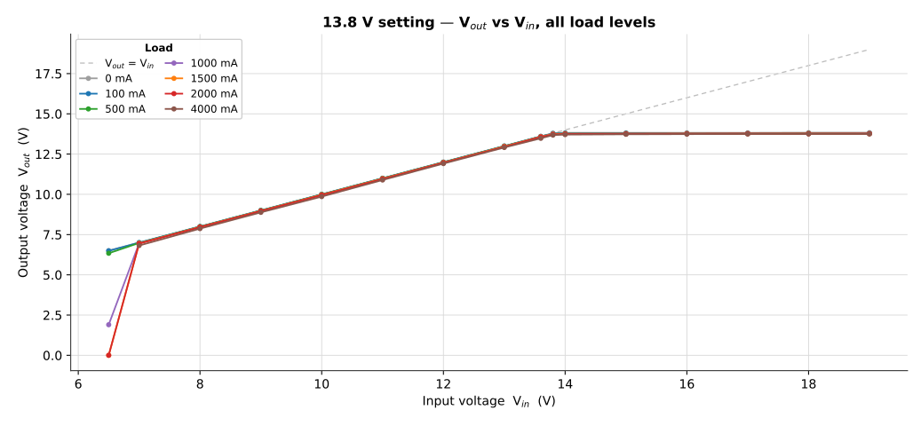
13.8 V setting — full input sweep, all load levels.
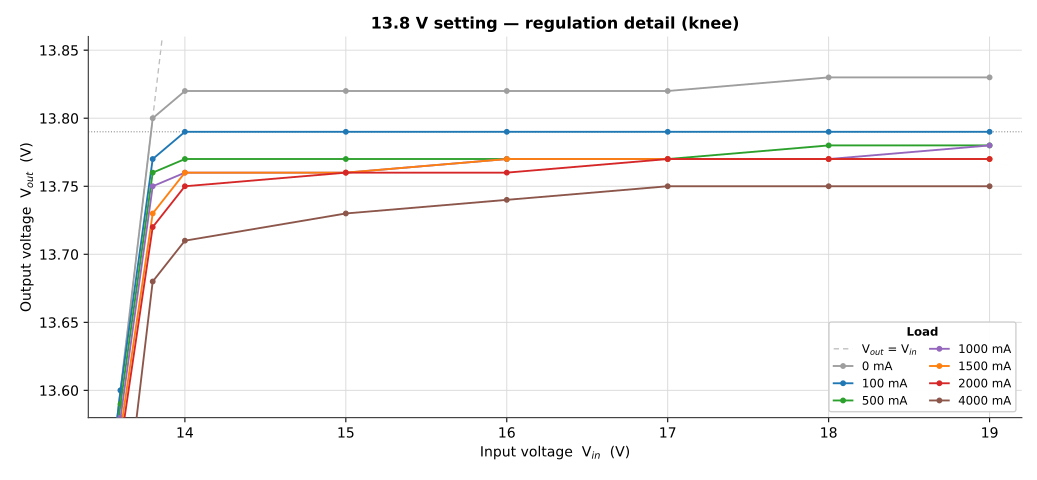
13.8 V setting — regulation knee in detail.
No-load float
With the output open and Vin above the setpoint, the output floats roughly 30–40 mV above its lightly-loaded value (visible as the 0 mA trace sitting highest in each zoom plot). It settles to the regulated value under even a light load. Trim the output with a light load (≈100 mA) attached rather than open-circuit.
Minimum input voltage
The regulator holds cleanly down to about 7 V at the tested loads. Below that, the minimum usable input rises with current: at 6.5 V the output is fine at 100–500 mA but collapses by 1–1.5 A (the steep drop on the left of each full-sweep plot). This is the pass device running out of gate drive at low input, not instability, and it sits below the normal operating range for any of the three output settings.
Thermal performance
The VLDO is a linear regulator, so the heat it dissipates is set primarily by the input–output difference times load current — (Vin − Vout) × Iload. Thermal data was taken at the 12 V setting with the included (compact) heat sink; for the same Vin − Vout the 9 V and 13.8 V settings should behave similarly. The practical consequence: 12 V in → 9 V out (3 V drop) runs as hot as 15 V in → 12 V out, and needs the same extra heatsinking (mounting to a case, or larger heat sink).
Heatsink temperature versus time key-down, supplied heatsink, 20 °C ambient:
| Load | Vin | 0 min | 1 | 2 | 3 | 4 | 5 | 6 | 7 | 10 |
|---|---|---|---|---|---|---|---|---|---|---|
| 1 A | 12 V | 23 | 23 | 24 | 24 | 24 | 24 | 25 | 25 | 26 |
| 2 A | 12 V | 23 | 26 | 29 | 31 | 32 | 34 | 35 | 35 | 37 |
| 1 A | 13 V | 23 | 31 | 37 | 40 | 44 | 46 | 47 | 48 | 51 |
| 1 A | 14 V | 23 | 37 | 50 | 59 | 65 | 70 | 73 | 76 | 78 |
| 1 A | 15 V | 23 | 47 | 66 | 78 | — | — | — | — | — |
| 1 A / 50% | 15 V | 23 | 36 | 45 | 51 | 56 | 60 | 62 | 63 | 65 |
Temperatures in °C. The 1 A / 50 % row simulates a QMX FT8 send/receive cycle (15 s on, 15 s off); it stabilised around 66–68 °C after ~20 minutes.
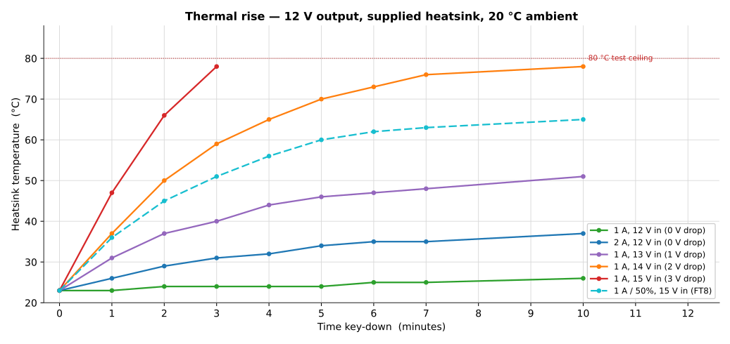
Thermal rise at 12 V output with the supplied heatsink, 20 °C ambient.
Practical guidance (supplied heatsink, 20 °C ambient):
- Up to ~1 V drop (e.g. 13 V in → 12 V out) at 1 A continuous key-down is comfortable (~51 °C).
- ~2 V drop at 1 A continuous runs hot (~78 °C) — fine for low-duty CW/SSB, marginal for sustained full-duty key-down.
- ~3 V drop (15 V in → 12 V out) exceeds the supplied heatsink at 100 % duty, but is fine at FT8 50 % duty (~66–68 °C, stable) — i.e. continuous FT8 is possible at 15 V in.
- Keeping Vin − Vout near 2 V (e.g. a 13.8 V supply for 12 V out) gives the best thermal margin. A larger heatsink widens all of the above; lower-duty modes (CW/SSB) tolerate higher ambient temperatures.
Output drift with temperature
Over a 23 → 80 °C heatsink rise (14 V in, 1 A), the regulated output drifted up by about +28 mV, roughly 0.23 % of Vout — consistent with the < 0.34 % figure noted in the design documentation. Most use will see a smaller rise; for QMX use this drift is inconsequential. (80 °C was a self-imposed test ceiling, a 57 °C rise above ambient.)
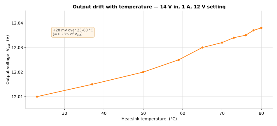
Output drift versus heatsink temperature, 14 V in, 1 A, 12 V setting.
Startup and shutdown
Startup behaviour was also examined: with a 13 V input at the 12 V setting, the output responds in approximately 150 µs with a clean, quick ramp and no detectable overshoot or other anomalous behaviour (within the resolution of the oscilloscope used). The input trace showed the expected dip as the board’s capacitors charged, attributed largely to inductance in the long supply leads used for the test. Shutdown was similarly clean, though much slower, governed by the discharge rate of the capacitors.
Relationship to the specification table
These bench results let several rows of the simulated spec table move toward hardware-verified status:
- Dropout, load regulation, line regulation — measured and consistent with simulated figures.
- Input range — operation confirmed down to 7 V at the tested loads, with a load-dependent minimum below that.
- Output drift with temperature — measured and consistent with the documented limit.
Still simulation-only, pending the dynamic measurements listed under Validation Status: loop characterisation (phase margin, unity-gain bandwidth, gain margin), PSRR, and output noise. None of these is addressed by the DC and thermal data above.
DC and thermal measurements: Stan Dye, KC7XE, June 2026. All values measured at the board terminals on a single V2 sample. Plots generated from Stan’s tabulated data. See the project README for design rationale, schematic lineage, and the full specification table.