M9OMS VLDO V1.1 vs V2 — Low-Dropout (LDO) Regulator Bench Comparison
A like-for-like bench comparison of the M9OMS VLDO V1.1 and V2 boards at the 12 V output setting. Both datasets are KC7XE bench measurements; this page uses the input voltages common to both runs. Each comparison is direct.
V2 characterisation is ongoing. The figures below are DC measurements on single samples of each board, taken at the board terminals. The dynamic measurements (transient response, loop characterisation, PSRR) listed under Validation Status are not addressed here.
Product page: M9OMS VLDO V2 — RF-quiet power supply for QRP Labs QMX
Scope and method
- Output setting. Only the 12 V setting is compared — which the V1.1 dataset covers. The 9 V and 13.8 V settings have no V1.1 data for comparison.
- Measurement point. All values are taken at the board terminals, with the supply raised under load to hold Vin, following the method in Bench Measurements. This removes lead-resistance drop, so the figures reflect the regulators rather than the wiring.
- Input range. Common Vin points only, data only collected upto 16 V.
- Metric. Load regulation, ΔVOUT = Vout(100 mA) − Vout(load), at 1 A and 2 A. For a QMX this corresponds to the receive-to-transmit step (≈100 mA to ≈1 A); the 2 A column covers higher-power use and margin.
Lower values indicate tighter regulation.
Results
ΔVOUT (mV) at each common input voltage, 12 V setting:
| Vin (V) | V1.1, 100 mA→1 A | V2, 100 mA→1 A | V1.1, 100 mA→2 A | V2, 100 mA→2 A |
|---|---|---|---|---|
| 8.0 | collapse † | 20 | collapse † | 50 |
| 9.0 | 300 | 20 | 1040 | 50 |
| 10.0 | 160 | 20 | 330 | 40 |
| 11.0 | 150 | 20 | 280 | 40 |
| 11.9 | 140 | 20 | 280 | 40 |
| 12.0 | 120 | 20 | 290 | 40 |
| 12.1 | 70 | 20 | 200 | 40 |
| 13.0 | 30 | 20 | 80 | 30 |
| 14.0 | 30 | 20 | 80 | 20 |
| 15.0 | 30 | 20 | 70 | 20 |
| 16.0 | 10 | 20 | 70 | 20 |
† At 8.0 V, V1.1 output collapses under load (Vout 1.1 V at both 1 A and 2 A); V2 maintains regulation at 8 V.
Two points on reading the table:
- In regulation (≈13–16 V), the 1 A figures are within the measurement floor. The two boards differ by no more than ±10 mV, and the single value favouring V1.1 at 16 V (10 vs 20 mV) sits at that resolution; it should not be read as a difference. The 1 A advantage appears only as Vin approaches the setpoint.
- At 2 A the difference is clear of the measurement floor across the range — approximately 2–3× lower ΔVOUT in regulation, improving further in the dropout region.
ΔVOUT vs input voltage
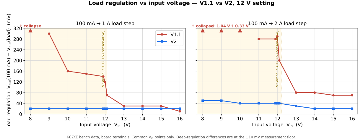
ΔVOUT, 12 V setting. The shaded band marks V2's conservative dropout estimate (Vin ≤ 12.1 V at 1 A, ≤ 12.2 V at 2 A); the V1.1 dropout boundary has not been characterised. V1.1 markers above the scale are off-chart; "collapse" indicates loss of regulation at that load.
V2 maintains a near-constant ΔVOUT across the voltage range — approximately 20 mV at 1 A and 40 mV at 2 A. V1.1 is comparable only above the setpoint, rapidly degrading as Vin falls, this is the range a battery occupies as it discharges.
Mechanism: output voltage vs input voltage
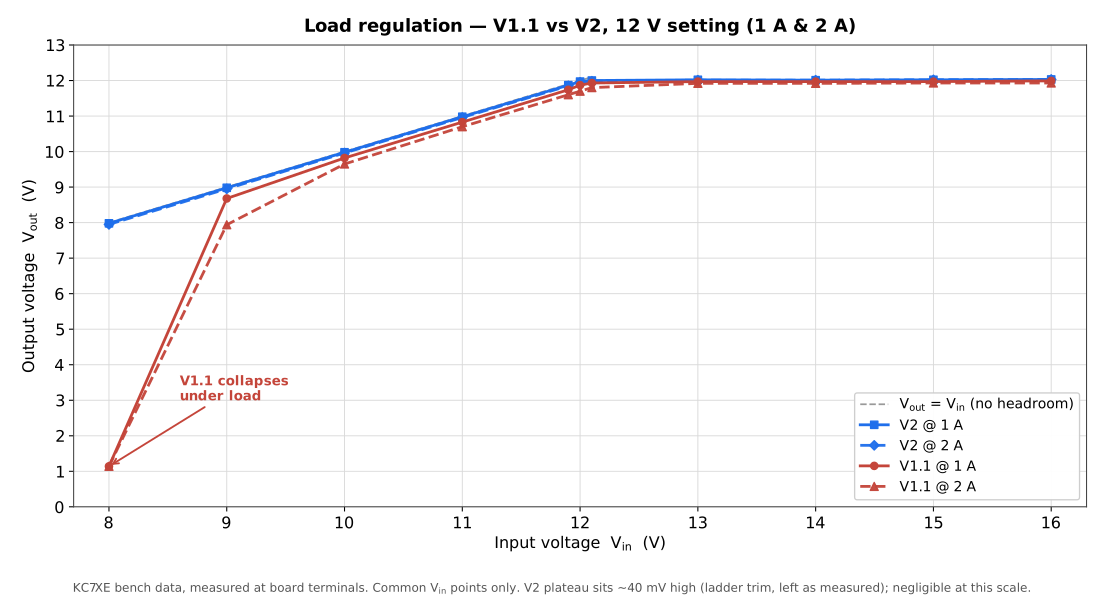
Output voltage versus input voltage, 12 V setting. V2 tracks the no-headroom line down to 8 V under load; V1.1 departs below ~9 V, collapsing at 8 V.
The ΔVOUT figures arise from two differences, both visible in the graphs.
Dropout-region behaviour. Below the 12 V setpoint a linear regulator can only pass Vin less its own dropout. V2’s lower dropout allows it to deliver close to the full input voltage at 1–2 A down to 8 V. V1.1 requires more headroom: under load its output departs from the input at around 11–12 V, deteriorating as it approaches by 8 V. For a 3S LiPo under transmit load, this determines how far down the battery discharge curve the supply remains usable before dropout affects the radio.
Pass-device conduction at higher current. At 2 A the V2 pass device drops less and is driven harder, so its 2 A ΔVOUT (~40 mV) remains close to its 1 A ΔVOUT (~20 mV). V1.1’s 2 A ΔVOUT is 2–3× the 1 A figure in regulation, increasing further in the dropout region as gate drive becomes insufficient — the same mechanism behind the loss of regulation at 8 V.
Regulation knee (11–14 V)
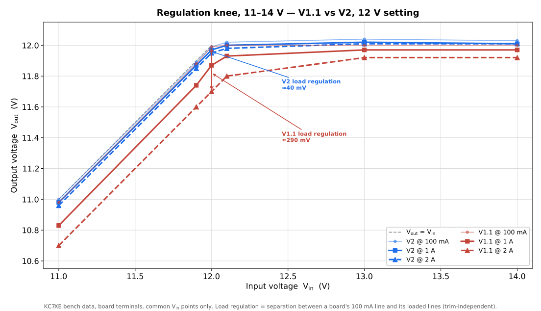
Regulation knee, 11–14 V. Each board's 100 mA, 1 A and 2 A traces are shown; ΔVOUT is the vertical separation between a board's light-load trace and its loaded traces, independent of trim.
Plotting all three load traces shows the behaviour in detail. V2’s 100 mA, 1 A and 2 A traces remain within approximately 40 mV of one another up to and through the knee, reaching the plateau by ~12.1 V. V1.1’s traces separate below ~12 V — at 12.0 V the 2 A output has fallen approximately 290 mV below the 100 mA trace — and the board does not fully settle until ~13 V. A 12 V output taken from a nominal 12 V battery operates within this window.
Summary
- In regulation: the two boards are comparable at 1 A; V2 shows approximately 2–3× lower ΔVOUT at 2 A.
- Approaching and below the setpoint: V2 maintains near-constant ΔVOUT (~20 mV at 1 A, ~40 mV at 2 A), while V1.1 degrades to several hundred millivolts and then loses regulation. This is the range relevant to battery operation.
- At 8 V, 1–2 A: V2 maintains output; V1.1 does not.
For the full V2 dataset (all three output settings, thermal, drift) see Bench Measurements; for the design rationale and the V1.1 → V2 change list see the project README.
Comparison data: Stan Dye, KC7XE. V1.1 and V2 measured by the same method, at the board terminals, single sample of each board. Plots generated from the tabulated data above.